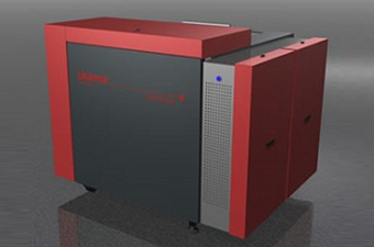
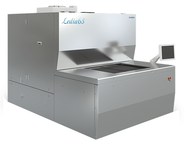
SCREEN Graphic and Precision Solutions Co. Ltd, is the leading manufacturer of Direct Imaging systems from Japan and has over 270 installations globally. LEDIA DI Direct Imaging system delivers field-proven high precision accuracy, reliability and throughput to PCB manufacturers with an estimated 70% market share amongst the largest global PCB manufacturers. LEDIA DI systems are now available in India exclusively through UCAMCO B.V, Belgium and Polar Instruments (Asia Pacific) Pte Ltd, Singapore. These systems are supported by Ucamco & Polar local network of highly skilled sales and support engineers.
3 simultaneous wavelengths
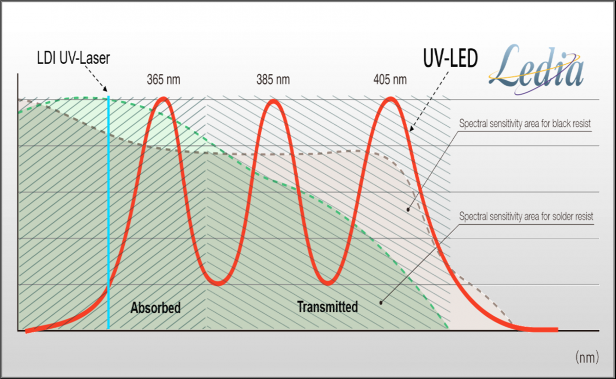
UV-LEDs with three wavelengths are now combined in the Ledia light source. The wave-length range from 350nm to 440nm enabling the energy diffuses optimally throughout the resist layer. The user can set each wavelengths power individually to achieve optimal imaging for resist or solder mask type. The result is high throughput and unrivalled quality that deliver 50µm solder mask dams without any noticeable undercut.

The combination of three wavelengths UV-LED allows different types of resists to be imaged using an optimal output ratio using wavelength modulation. Compared to a standard direct imaging system, the LEDIA enables manufacturers to pursue even higher imaging quality. The system supports cutting-edge technologies, including a high-precision auto-focus function and alignment algorithms that compensate for various types of substrate distortion.

Low operational cost
The adoption of UV-LED technology as a light source results in considerable lower consumable cost compared to conventional laser direct imaging systems. Also the LED’s are only active when physically imaging panels, resulting in an even longer LED life time.
Cost Cutting
- No mask making costs.
- Rationalization of manpower by simplified mask manufacturing process.
- Enhanced production yields.
- Better Registration
- No repeat defects
Faster Delivery Times
- Shortened turnaround time achieved by simplified manufacturing.
- Easy and flexible process control.
High-Value added Product
- High precision and high accuracy patterns.
- Easy management or control on individual board.
- Easy Operation. (For skill-Less Operator)
Highest productivity for solder mask
UV-LED technology in combination with multi wavelength LEDs delivers high throughput with the highest quality for your solder mask applications. The different wavelengths have peaks in both the absorbed and the transmitted wavelength areas of the spectrum of the solder mask inks. This allows even polymerization at the top as well as the bottom of the solder mask layer, resulting in a fully polymerized layer with optimal adhesion to the substrate.

Download Brochure
